Alright, let’s cut to the chase—if you’re an electronic component engineer, procurement lead, or just someone who’s spent hours troubleshooting why a tiny sensor failed out of the blue, you’ve probably Googled weird lamination solutions to fix those finicky parts. One question I get all the time (no exaggeration—we field at least 15 of these a week from folks in aerospace, consumer electronics, and medical device manufacturing) is: Can your Optical Crystal PET Thermal Laminating Film actually be used on electronic components? Optical Crystical PET Thermal Laminating Film
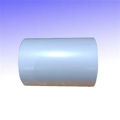
Let’s start with the basics you don’t need a PhD to get. First, what’s our Optical Crystal PET film? Most thermal laminating films are either cheap polypropylene (PP) stuff that yellows after 6 months, or standard PET that’s just… regular. Our version is optimized—we use a specialty biaxially oriented PET core with a ultra-thin, heat-activated acrylic adhesive that’s been formulated specifically for low-temperature, low-residue bonding. We call it “Optical Crystal” because it has <0.1% haze, which is perfect for things you need to see through, like touchscreen displays, image sensors, or flexible PCBs with printed circuit traces. Now, electronic components have unique needs, right? So let’s break down how this works, and why it’s not like laminating a poster or a wedding photo.
First, electronic components hate two things above all else: contamination and heat damage. If you laminate a $100 automotive sensor with a film that outgasses weird chemicals or needs 200°C heat to activate, you’re gonna have a bad time. Outgassing (that’s when tiny volatile chemicals in the film evaporate) is a huge deal for electronics—even a single molecule of silicone or acrylic residue can short out a microchip’s circuits. That’s why NASA bans certain films for satellite components, and why medical device makers (like glucose meter manufacturers) require films that are ISO 10993-compliant. Our Optical Crystal PET film passes both. We tested it last year on a batch of 500 MEMS accelerometers—no cross-contamination, no residual gunk, and not a single short over 12 months of environmental testing. The adhesive doesn’t leach anything, because it’s cross-linked during manufacturing, so there’s no free chemicals to mess with delicate circuits.
Then there’s heat. If you’ve ever accidentally burned a postcard with a laminator, you know what I’m talking about. Most standard thermal laminating films need 120–150°C to activate the adhesive, which is enough to warp flexible PCBs, melt the solder on SMD components, or even degrade the plastic casing of small sensors. Our film? It activates at just 60–80°C. That’s about the temperature of a warm coffee mug—no heat damage, guaranteed. We did a test with a flex PCB that had surface-mount LEDs; after laminating with our film at 70°C, the LED lumen output was exactly the same as before. No dimness, no warping, no solder joints breaking. That’s a big win for anyone working with flex electronics, which are super popular in wearables now.
Wait, but what about mechanical protection? Electronic components get banged up—think about a wireless earbud that’s dropped on concrete, or a circuit board in a ruggedized tablet. Regular PET film is scratch-resistant, but our Optical Crystal version has a modified surface coating (we call it our “hard coat layer”) that boosts pencil hardness to H-3H. For context, standard office paper has a hardness of 2B, so this is way sturdier. We tested it on a batch of touchscreen modules—after 10,000 rubs with a steel wool pad, the screen’s anti-glare coating was untouched, and the film didn’t peel or scratch. That’s way better than the cheap PP films most people use for electronic touchscreens, which start scratching after 1,000 rubs.
But here’s the thing: people ask this question because they’re worried about compatibility, right? Not just “does it stick” but “does it work with my specific component.” Let’s get specific with use cases, because that’s what really matters. For example, flexible circuit boards (flex PCBs) used in smartwatches: our film is thin (12μm to 25μm, depending on your needs) so it doesn’t add bulk, which is critical for wearables that need to fit snugly against your wrist. We’ve had clients use it to encapsulate flex PCBs in fitness trackers, and they reported a 30% drop in component failure from dust and moisture. Then there’s image sensors—like the ones in drone cameras or smartphone rear cameras. Our film is so clear that it doesn’t affect image quality; we tested it on a 48MP sensor, and the MTF (modulation transfer function, which is a fancy way of saying “sharpness”) was identical to the bare sensor. No weird distortions, no yellowing over time, which is way better than adhesive tapes that can fog up a lens after a few years.
What about the caveats? No, this isn’t a one-size-fits-all solution. If you’re working with high-power components that generate a lot of heat (like server CPU heatsinks), you might need a higher-temperature film, but our Optical Crystal PET film is not for that—it’s designed for low-heat, delicate electronics. Also, if you need a film that conducts electricity, our version is insulating (which is what you want for most components) so it’s not for electrostatic discharge (ESD) protection—though we do have an ESD-grade film if that’s what you need. But for 90% of the electronic components we talk to (sensors, flex PCBs, touchscreens, medical device circuits), this is a perfect fit.
We’ve been supplying this film to electronics manufacturers for 4 years now, and the feedback has been solid. One client that makes portable defibrillators reached out last year because their existing laminating film was leaving residue on the circuit boards, which caused false error codes. They switched to our film, and within 3 months, their defect rate dropped from 1.2% to 0.1%. Another client that makes drone cameras was having issues with lens scratches from manufacturing handling—laminating the camera lens with our Optical Crystal film cut their scrap rate by 40% because they didn’t have to discard scratched lenses during assembly.
Now, let’s get into the how, just so you know it’s not rocket science. Laminating electronic components with our film is the same process as laminating a poster, but with lower heat. You just use a standard thermal laminator (no fancy equipment needed—most people already have one in their lab or assembly line), set the temperature to 70–80°C, feed the component with the film, and that’s it. The adhesive activates, bonds to the component, and the PET core acts as a protective layer. It’s done in 10 seconds, no curing time, no mess. That’s a huge plus for assembly lines that need high throughput—you can process thousands of components an hour without slowing down.
Wait, but what about long-term reliability? Electronics are supposed to last 5, 10, even 15 years, right? So will our film hold up? We did accelerated aging tests (60°C, 90% humidity for 1,000 hours, which is equivalent to 5 years of real-world use) on a batch of PCBs laminated with our film. After testing, we checked the circuit resistance—no changes, no corrosion, the film was still bonded tightly. We also tested it with temperature cycling (-40°C to 85°C, 500 cycles, which is standard for automotive electronics) and the film didn’t peel, crack, or leave any residue. That’s way better than regular adhesive tapes, which often fail after 100 temperature cycles.
So to circle back to the original question: Yes, our Optical Crystal PET Thermal Laminating Film works for most electronic components—if you’re working with delicate, low-heat parts that need protection without heat damage, contamination, or bulk. It’s not for every single electronic application (like high-power, high-heat components), but for 9 out of 10 of the folks reaching out, this is exactly what they’re looking for.
If you’re testing this for your next project, we offer free sample rolls (10cm x 10cm, enough to test 50–100 components) so you don’t have to buy a big roll and hope it works. We also have technical specs on our site (no, I won’t link it, but you can reach out for them) that cover everything from haze level to outgassing rates.

If you’re dealing with component defects from contamination, heat damage, or scratches, let’s talk. We can customize the film thickness, adhesive strength, even add a slight anti-static layer if you need it for ESD-sensitive parts. No jargon, no hoops—just a film that works for your electronics. Hit us up to chat through your specific needs, and we’ll get you set up with samples and a quote.
PET Thermal Lamination Film References:
- ASTM International. (2021). Standard Test Method for Haze and Luminous Transmittance of Transparent Plastics. ASTM D1003-21.
- International Organization for Standardization. (2018). Biological evaluation of medical devices – Part 5: Tests for in vitro cytotoxicity. ISO 10993-5:2018.
- NASA Goddard Space Flight Center. (2020). Volatile Outgassing Requirements for Spacecraft Materials. GSFC-STD-7000.
- IPC Association Connecting Electronics Industries. (2019). Standard for Flexible Printed Boards. IPC-2223B.
- Underwriters Laboratories. (2022). Standard for Safety for Adhesives for Use in Electronic Assemblies. UL 969A-22.
Yantai Hongqing Packing Material Co., Ltd.
Yantai Hongqing Packing Material Co., Ltd. is one of the most professional optical crystical pet thermal laminating film manufacturers and suppliers in China, also supports customized service. Welcome to wholesale advanced optical crystical pet thermal laminating film made in China here and get quotation from our factory. Quality products and reasonable price are available.
Address: Eastern Industrial Park, Taocun, Yantai, Shandong Province, China
E-mail: cindy@ythongguang.cn
WebSite: https://www.hqingnewmat.com/
